Printed
Electronics

High-performance and cost-effective
High-performance
and cost-effective
The interest in printed electronics is not new. For years, the electronics industry has anticipated a market disruption that, for the most part, has yet to materialize. The goal is to start replacing the traditional, concentrated, capital-intensive, subtractive manufacturing processes with a more distributed, capital-efficient manufacturing base that creates electronics with additive printing processes. We’re here to help.
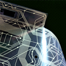
New functionality, higher performance and new form factors all have been driving toward the emergence of printed, flexible electronics that will require new material sets of conductive, semiconductive and dielectric inks. This would allow transistors to be printed for anything from simple RFID tags to fully functional display backplanes.
Critical to the success of these applications is the need to match performance to cost and functionality. We believe Promethean’s technology lends itself incredibly well to producing the critical ingredients so ink formulators can produce high-performance and cost-effective conductive and dielectric inks. Nanoparticles enable milder processing conditions, such as lower sintering temperatures, compared with bulk materials.
Printed electronics typically include these families:
- Conductors (RFID, for example)
- Semiconductors (transistors, switches, diodes)
- Dielectrics (lower-voltage applications, capacitors)
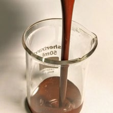
Copper Nanodispersion
- Functional pigment for printed inks — printed conductive tracks, ultrafine screen features, flexible substrates
- For printed components such as fully printed PCBs and antennas
- Nano-copper (approximately 100 nm)
- Conductive metal
- Cost-effective alternative to silver
- Contains only copper and an antioxidant
- Cost-effective process due to low CAPEX and OPEX costs
- Non-oxidised material
- Standard 50 or 65 wt% Cu available in a range of solvents
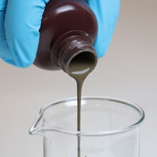
Silver Nanodispersion
- Functional pigment for printed inks — printed conductive tracks, ultrafine screen features, flexible substrates
- For printed components such as fully printed PCBs and antennas
- Nano-silver (approximately 50 nm)
- Highly conductive metal
- Used for higher demanding applications
- Water-based dispersion
Barium Titanate Nanodispersion
- Dielectric material for capacitors, printed components (such as thin film transistors and diodes), piezoelectric material
- Small primary particle size (less than 20 nm)
- High crystallinity
- Water-based dispersion
Nickel Nanodispersion
- Non-oxidised material
- High crystallinity
- Standard 25 wt% Ni available in water or ethanol
We’re ready to
discuss your next
project
We’re ready to discuss your next project

Have a technical challenge? Connect with our team of experts to see what we can bring to your product application.